
Description

PCB Stack-Up: Plan, Design, and Manufacture
Designing a 6-Layer PCB Stackup for Enhanced EMC, Blog

Prototypes - PCB Prototype the Easy Way - PCBWay
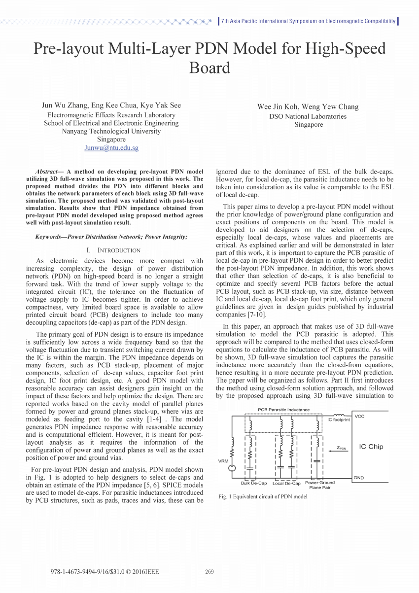
PDF) Pre-layout multi-layer PDN model for high-speed board

a The effect of air jet velocity on the moisture content of paper

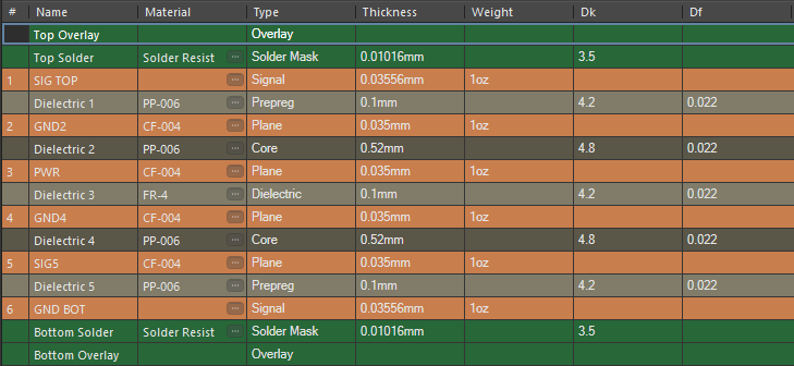
Guide to Multilayer PCB Layer Stackup and thickness - JHYPCB

Normalized shear modulus reduction of GF/EP cross-ply laminate

Design PCBs for EMI, part 2: Basic stack-up - EDN Asia

Top layer and bottom layer of test board

Normalized shear modulus reduction of CF/EP cross-ply laminates
8 Layer PCB Manufacturer– Everything You Need to Know


You may also like

Solid Plush Over The Knee Socks, Thermal Thickened Winter Knee High Stocks, Women's Stockings & Hosiery

50pcs Breathable Disposable Knickers Disposable Underpants Disposable Underwear

Weight Lifting/Power Lifting Belt Suede Double Prong Leather Belt - 4 Inches Wide, 10 MM - Maximum Support & Protection - Power Lifting Strap Inzer

NIKE FE/ NOM GIRLS SPORTS BRA SIZE MEDIUM BV2780-682 PINK 10-12 YEARS TRAINING
$ 7.99USD
Score 4.5(186)
In stock
Continue to book
You may also like
Solid Plush Over The Knee Socks, Thermal Thickened Winter Knee High Stocks, Women's Stockings & Hosiery
50pcs Breathable Disposable Knickers Disposable Underpants Disposable Underwear
Weight Lifting/Power Lifting Belt Suede Double Prong Leather Belt - 4 Inches Wide, 10 MM - Maximum Support & Protection - Power Lifting Strap Inzer
NIKE FE/ NOM GIRLS SPORTS BRA SIZE MEDIUM BV2780-682 PINK 10-12 YEARS TRAINING
$ 7.99USD
Score 4.5(186)
In stock
Continue to book
©2018-2024, paramtechnoedge.com, Inc. or its affiliates