
Description
This case study focuses on the challenges and solutions that we implemented to design complex HDI boards with stacked vias.

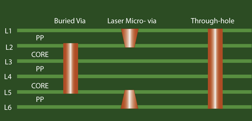
Case study: 8 and 14-layer HDI with Stacked Vias
How HDI Boards Can Be More Economical
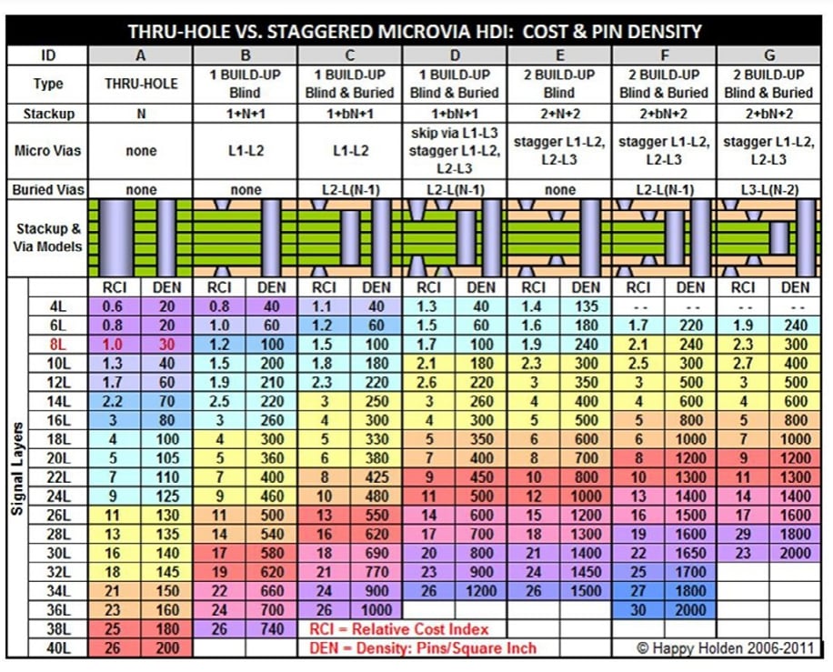
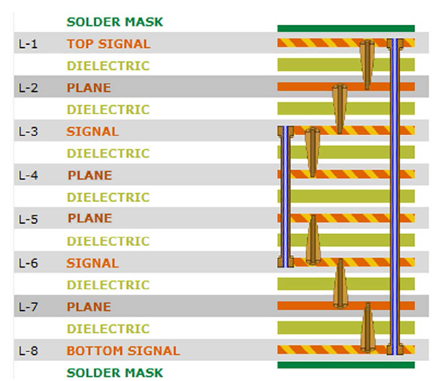
Designing Staggered and Stacked Vias

Signal Integrity Characterization of Via Stubs on High-Speed DDR4 Channels, 2020-05-14

Understanding Proper PCB Design (Part 2) - Circuit Cellar
High Density Interconnect HDI PCB Manufacturer - Jhdpcb
a) SEM-micrograph of the top part of a 10 layer stacked via after

Top 18 HDI PCB Manufacturers In the world - RAYPCB
14 Layer PCB HDI Vias in Pad BGA

Explain Like I'm a Designer: ELIC PCB and HDI Routing, HDI Design

An in-depth analysis on PCB stackup – PCB HERO
HDI board stack-ups – PCB HERO
Related products


You may also like

Cotton and Lace Trim Cheeky Panty - Black

30AA Bras Buy Size 30AA Bras at Betty and Belle Lingerie

Women Underbust Neoprene Sport Girdle Corsets Cincher With Zipper, Adjustable Workout Sweat Waist Trainer Corset Trimmer , Double Belt Hourglass Body Shaper - China Cincher and Waist Cincher price

Simone Perele Karma Triangle Lace Bralette 12V250 – Cherchez La Femme Boutique
$ 26.00USD
Score 4.9(190)
In stock
Continue to book
You may also like
Cotton and Lace Trim Cheeky Panty - Black
30AA Bras Buy Size 30AA Bras at Betty and Belle Lingerie
Women Underbust Neoprene Sport Girdle Corsets Cincher With Zipper, Adjustable Workout Sweat Waist Trainer Corset Trimmer , Double Belt Hourglass Body Shaper - China Cincher and Waist Cincher price
Simone Perele Karma Triangle Lace Bralette 12V250 – Cherchez La Femme Boutique
$ 26.00USD
Score 4.9(190)
In stock
Continue to book
©2018-2024, paramtechnoedge.com, Inc. or its affiliates