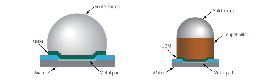
The bond pad redistribution layer (polyimide 1) and the under bump

Description

PDF) Embedding of Thinned RF Chips and Electrical Redistribution Layer Characterization

Fan-Out Packaging Gets Competitive

The bond pad redistribution layer (polyimide 1) and the under bump

Warren FLACK, Vice President, PhD

US6660624B2 - Method for reducing fluorine induced defects on a bonding pad surface - Google Patents
Electromigration Performance Of Fine-Line Cu Redistribution Layer (RDL) For HDFO Packaging

Fan-Out Packaging Gets Competitive
Warren FLACK, Vice President, PhD

CN111108144A - Curable polyimide - Google Patents

Chip Scale Packaging Helps Portable Medical Devices Save Size and Weight

Polymers, Free Full-Text

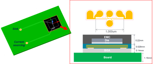
Fan-In Wafer/Panel-Level Chip-Scale Packages
Tech Brief: Primer on Packaging
Related products


$ 14.50USD
Score 4.6(793)
In stock
Continue to book
$ 14.50USD
Score 4.6(793)
In stock
Continue to book
©2018-2024, paramtechnoedge.com, Inc. or its affiliates