pcb - Connecting pads with the same functionality belonging to one chip - Electrical Engineering Stack Exchange

I have a question about routing style of pads with the same functionality belonging to one chip. I draw a picture in Paint (fictional IC; let it be the SOIC8 footprint). GND is only as example (it
What is a pad/padstack used for in a PCB layout? - Quora
pcb design - Same net overlapping pads ok? - Electrical Engineering Stack Exchange
What is a pad stack in PCB? - Quora
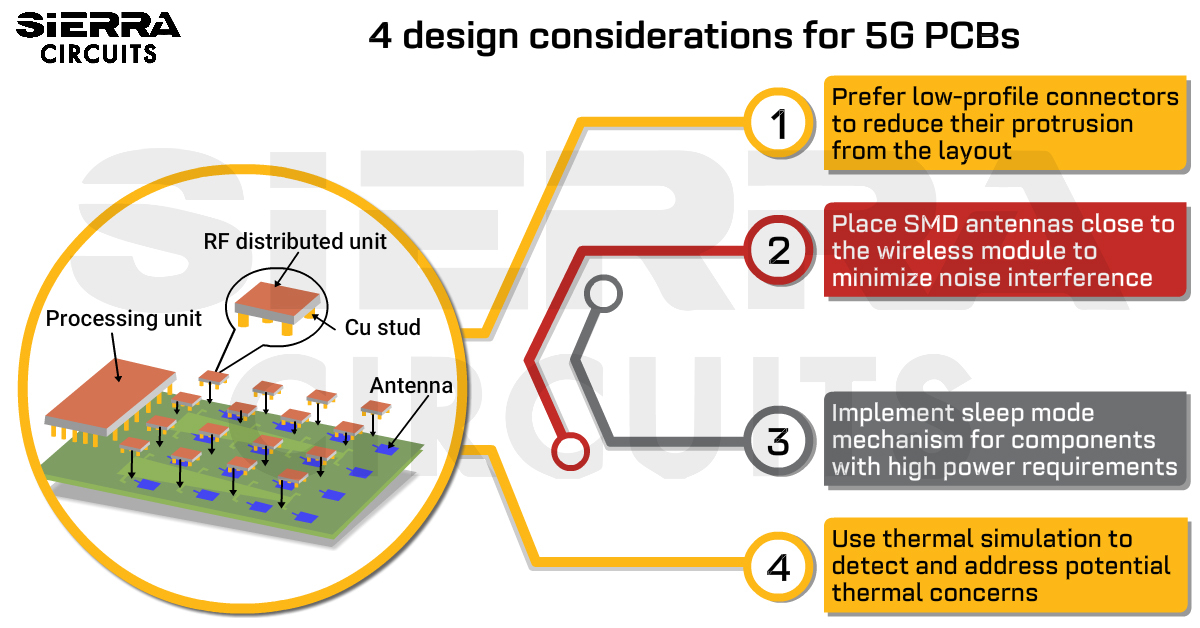
How to Design PCBs for 5G Wireless Applications

Flip-Chip - Semiconductor Engineering

High-TECH PCB Reverse Engineering Services - RAYPCB

Raspberry Pi - Wikipedia
pcb - Using oblong / rounded surface mounted pads for chip resistors, capacitors and inductors - Electrical Engineering Stack Exchange

Application and Use of PCBs - PCB Power

High-Bandwidth Memory (HBM) - Semiconductor Engineering

Power Pcb Design, Electrical Printed Circuit Board Design And Layout For Power Supply
Common PCB Assembly Defects You Should Know, Industry Expert

)