The complete guide to PCB pad :types, size, spacing, repair and

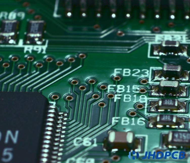
Soldering is one of the most important processes in PCBA processing. On printed circuit boards, electrical connections to all components are made via PCB pads. The PCB pads are a very critical part of the PCB that determines where components are soldered on the PCB.The size, shape, and position of pads in a PCB directly depend on the manufacturing quality of the board. Today we will take a look at the PCB pad in SMT soldering.
Soldering is one of the most important processes in PCBA processing. On printed circuit boards, electrical connections to all components are made via PCB pad.
What Types Of Holes Are There In The Pcb Manufacturing Process? - Jhdpcb

PCB Thermal Pad : Guardians of Electronic Heat Regulation - IBE Electronics

LG Innotek launched the world's thinnest semiconductor package substrate - IBE Electronics

PCB connector : definition, types, and how to choose and identify - IBE Electronics
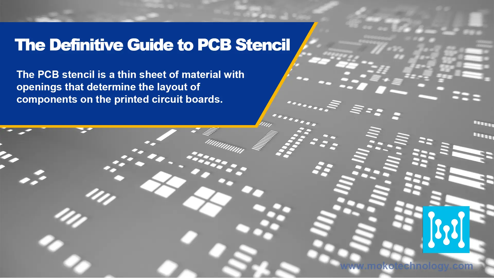
The Definitive Guide to PCB Stencil: Everything You Need to Know

PCB connector : definition, types, and how to choose and identify - IBE Electronics

How To Repair Damaged /Missing PCB Pads INVISIBLE Fix, 45% OFF

PCB Pad-to-Pad Spacing and Its Impact on DFM - VSE

Energy storage PCB market embraces a broad development space under soaring new energy trends - IBE Electronics